AI-driven analytics has transformed semiconductor manufacturing economics: reducing lead times by up to 30%, increasing production efficiency by 10%, and cutting CapEx by 5% through smarter process optimization, according to research by McKinsey.
Whether in the 1990s, 2000s, or 2020s, fabs have always wanted to streamline end-to-end processes of designing and manufacturing semiconductors for improving productivity and profitability. The application of advanced analytics, Machine Learning (ML), and Artificial Intelligence (AI) that save time and costs is not enough.
Your Artificial Intelligence (AI) in semiconductor manufacturing must unlock new approaches to yield and throughput improvement. And they should also complement your traditional yield management methods to save $38 billion annually, as per McKinsey.
Decades ago, chip manufacturing relied on manual processes and basic statistical methods. Today, with AI, ML, and advanced analytics available, many companies still struggle to capture their full potential across operations.
Currently,
- Lead times for bringing integrated circuits to market rise with each node.
- New product introduction takes about 12-18 months of iterative debugging due to increased complexity in design and manufacturing processes.
- Semiconductor manufacturers spend about 30% of CapEx on assembly and functional testing that does not add value.
Those numbers lead to yield losses in the semiconductor value chain. Will AI, data, and advanced analytics provide the solutions semiconductor businesses need? This blog post answers that question and describes how advanced analytics contributes to $38 billion annual savings to semiconductor manufacturers.
What is semiconductor yield optimization and how does it impact productivity?
Semiconductor yield improvement refers to maximizing the percentage of functional chips produced from each wafer during manufacturing. It’s the most critical metric determining fab profitability.
Why yield loss is expensive for semiconductor manufacturers:
- A 300mm wafer at advanced nodes costs $5,000-$17,000 to produce
- Each wafer holds 500-1,000 chips, depending on the die size
- Every defective chip on that wafer represents pure loss
The effects of poor yield add up fast. It includes direct scrap losses, engineering analysis time, production schedule delays, and missed customer commitments, all of which compound the initial defect event.
Moreover, the yield loss intensifies at advanced nodes. Today’s 7nm, 5nm, and 3nm processes involve 500-1,000 individual processing steps. Every step adds a new defect risk. For example, a contamination event during step 247 may not manifest as a visible defect until step 612. By that time, hundreds of wafers may have been affected, resulting in productivity loss. As process complexity grows at smaller nodes, traditional yield management methods cannot keep up with the speed and variability of modern fabs.
Why traditional yield management methods cannot keep pace with modern fabs
Traditional methods rely on statistical process control, sampling inspection protocols, and engineers manually reviewing control charts. Suppose production yield drops. To find the reasons, teams compare recent process changes, assess equipment logs, and run designed experiments. This approach works well for simple, stable processes with few variables.
Take an example of plasma etch complexity. Chamber effects on critical dimensions (CD) can vary by several nanometers chamber-to-chamber on the same tool. At 40nm nodes, this variation was manageable with traditional methods. But as geometries shrink to 7nm and below, those same variations now consume most of the available process margin.
Three main reasons make traditional methods insufficient:
Traditional methods fall short in handling complex semiconductor manufacturing challenges due to the following reasons:
-
Data volume overwhelms manual analysis
Engineers cannot keep up with data streams from thousands of tools simultaneously. By the time patterns emerge in daily or weekly reviews, hundreds or thousands of wafers may already be affected.
-
Hidden root causes
Standard correlation methods often miss warning signs as they cannot process non-linear interactions or detect outliers in data. Certainly, yield issues involve interactions between multiple process steps, equipment conditions, and material variations. Therefore, root cause analysis stays hidden or takes time to find out.
-
Speed determines cost impact
Research by Deloitte states that reducing the time required to plan maintenance by 20-50% can increase equipment availability by 10–20%. And manual investigation cycles, which can take weeks in yield improvement, cannot compete with artificial intelligence in semiconductor manufacturing systems that flag anomalies in real-time, enabling immediate corrective action.
How does advanced analytics improve semiconductor yield improvement
Advanced analytics in semiconductor yield optimization replaces guesswork with evidence derived from data correlation. Instead of waiting for defects to appear in later stages of production, real-time analytics in semiconductor fab continuously monitor process signatures and predict outcomes before quality issues emerge.
What insights do real-time analytics in the fab reveal?
A typical fab generates terabytes of data daily from equipment sensors, metrology tools, inspection systems, and test results. This data stream contains patterns that highlight:
- Which process parameter combinations produce optimal results
- How does equipment behavior change before failures occur
- Where yield losses originate within the manufacturing flow
- Which product types demonstrate the greatest sensitivity to specific variations
One key change for yield optimization is shifting emphasis from periodic in-line metrology to continuous real-time monitoring. Waiting until a process finishes to measure results slows production and delays corrective action.
Real-time sensor data, like chamber pressure, gas flow, temperature, RF power, and plasma impedance, gives actionable insight into how processes are running. This allows engineers to maintain tight mean and standard deviation control across run-to-run, chamber-to-chamber, tool-to-tool, and site-to-site variations.
For example, AI in semiconductor manufacturing can detect subtle process issues long before they appear as defects, as shown in the table. ML algorithms recognize a 0.3% drift in RF power during step 156, combined with a 0.5°C temperature variation in step 243, creates a defect signature that appears 400 steps later during final metrology.
| Step | Tool/Stage | Observation | Impact |
|---|---|---|---|
| 156 | Plasma etch tool | 0.3% RF power drift identified through real-time sensor monitoring | Contributes to defect signature |
| 243 | Chemical-mechanical planarization | 0.5°C wafer temperature variation revealed by inline thermal sensors | Amplifies defect risk |
| 600+ | Final metrology | Defect appears, detectable using computer vision techniques | Hundreds of wafers affected if not corrected |
| Action | – | Adjust process parameters immediately | Prevents defect propagation |
Advanced analytics in semiconductor yield optimization identifies correlations in near real time and that humans cannot detect with ease. These systems process thousands of variables simultaneously, detecting subtle interactions between temperature uniformity, pressure stability, gas composition, and timing parameters that collectively influence yield outcomes.
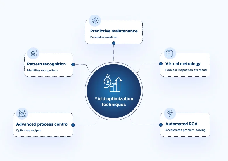
Which are the top five analytics techniques that improve yield and increase profitability
Semiconductor yield improvement relies on extracting actionable insights from massive amounts of process and equipment data. Advanced analytics techniques help identify inefficiencies, predict failures, and optimize operations to maximize output.
-
Predictive maintenance through equipment health monitoring
What is predictive maintenance in semiconductor manufacturing?
Equipment degradation happens gradually. A plasma etch chamber that performed perfectly six months ago now leaves polymer residues, causing defects. Changes are subtle, such as slight chamber pressure baseline increases, minor gas flow variations, and gradual RF power coupling efficiency drift.
How predictive maintenance works:
Sensors monitor vibration patterns, temperature profiles, pressure consistency, gas flow rates, and power consumption metrics. Machine learning models establish normal operating ranges for each parameter based on historical performance data. When values drift outside acceptable bounds, the system alerts maintenance teams to intervene proactively.

The operational results of predictive analytics:
- Scheduled maintenance replaces emergency downtime
- Equipment remains within specification ranges for extended periods
- Unplanned downtime reduces significantly
- Tool productivity increases without capital investment
-
Virtual metrology for reduced inspection overhead
What is virtual metrology?
Physical metrology is expensive and time-consuming. High-volume fabs face a fundamental trade-off: measure every wafer and sacrifice throughput, or sample periodically and risk missing quality excursions.
Virtual metrology yield optimization resolves this dilemma by predicting measurement results using process data instead of physical inspection. Machine learning models learn relationships between equipment sensor data during processing and subsequent metrology results.
How virtual metrology works:
The technique functions by training models on historical data where both process parameters and actual metrology measurements exist. Once trained adequately, these models predict film thickness, critical dimensions, plasma impedance, or other metrology targets based solely on equipment sensor readings and recipe parameters.
Benefits of virtual metrology:
- Reduces metrology frequency by half while maintaining quality control standards
- Saves time and cost, particularly for inline metrology operations that constrain throughput
- Improves cycle time while maintaining product quality assurance
-
Automated root cause analysis for accelerated problem resolution
Why is fast root cause analysis critical and how does it work?
When yield drops unexpectedly, every hour of investigation means more wafers processed under sub-optimal conditions. Traditional root cause analysis typically requires 3-7 days for moderately complex issues.
AI-driven automated root cause analysis compresses this timeline to minutes by continuously monitoring all process data, equipment events, and quality outcomes across the fab.
Real-world example: Yield on a critical memory product drops 3% overnight.
The automated system completes initial analysis in eight minutes, identifying:
- Failing units all processed through Chamber 4 on Etch Tool 7 during a six-hour window
- Sensor data shows subtle helium flow drift correlating with defect density
- Maintenance records indicate recent PM cycle completion
- Root cause: Incomplete chamber seasoning after maintenance
Engineers act immediately, pulling affected wafers and implementing additional seasoning cycles. Instead of days of investigation and hundreds of additional affected wafers, the issue resolves within hours.
This acceleration represents one of the most immediate benefits of yield analytics tools for semiconductor implementation.
-
Advanced process control through multi-variable optimization
How does AI optimize complex processes?
Modern semiconductor processes contain hundreds of controllable parameters, each influencing multiple output characteristics. Finding optimal settings manually proves impractical as combinatorial complexity overwhelms designed experiment approaches.
Machine learning algorithms explore parameter space far more efficiently, conducting virtual experiments continuously during production and adjusting multiple parameters simultaneously to learn optimal combinations.
Key difference from traditional control:
Instead of maintaining fixed recipe setpoints, advanced process control (APC) systems adjust parameters dynamically based on real-time equipment state, material characteristics, and quality targets, within carefully defined safe operating boundaries.
Results:
- Process capability indices (Cpk) improve marginally
- Yield gains of 2-5% in well-controlled processes
- Continuous re-optimization as conditions change, maintaining peak performance automatically
-
Pattern recognition in wafer-level defect maps
How do defect patterns reveal their sources?
Defects cluster in patterns that reveal their source with remarkable consistency:
- Edge defects suggest handling issues during wafer transfer operations
- Radial patterns indicate process uniformity problems within reaction chambers
- Random distribution points to particulate contamination from ambient sources
AI in semiconductor yield systems classifies defect patterns automatically and links them to specific causal factors. Engineers see not merely where defects occur but why they occur, based on spatial signatures that match known failure modes from historical production data.
The system correlates automatically:
- Which equipment chambers processed these wafers?
- What were the process conditions?
- When did the last preventive maintenance occur?
- Were there equipment alarms or parameter excursions?
Multi-factor interactions invisible to traditional analysis become obvious to machine learning algorithms trained on sufficient historical data.

What business impact should you expect across KPIs with AI in semiconductor yield?
Advanced analytics in semiconductor yield optimization turns real-time data into actionable insights. This enables manufacturers to improve yield, reduce costs, accelerate time-to-market, and make faster, more informed decisions.
Key performance improvements where you can realize semiconductor yield improvement:
-
Faster yield ramps
New products reach target yield much faster when analytics guide process optimization from the start of production ramp. This acceleration directly impacts time-to-revenue for new product introductions.
-
Reduced scrap costs
Early defect detection prevents good wafers from being processed alongside defective ones, cutting scrap by 10-20%. At advanced nodes where wafer costs exceed $16,000, these savings accumulate rapidly.
-
Higher equipment utilization
Predictive maintenance reduces unplanned downtime significantly, keeping tools productive for longer periods. This increased availability directly translates to higher fab output without capital investment.
-
Improved cycle time
Fewer process holds and faster troubleshooting mean wafers move through the fab 10-15% faster. This reduction in cycle time improves customer responsiveness and reduces work-in-progress inventory carrying costs.
-
Lower engineering overhead
Automated analysis reduces the time engineers spend investigating routine issues. This allows them to focus on strategic improvement projects rather than firefighting daily production problems.
-
Measurable ROI
Time can vary for getting results after implementing yield analytics tools across semiconductor operations. Any company can report a saving of $12 million in 18 months. These savings can come from reduced scrap, better equipment uptime, and faster product ramps, demonstrating measurable return on investment.
What does the future of yield optimization look like with AI and advanced analytics?
Artificial intelligence in semiconductor manufacturing is progressing toward closed-loop control capabilities. Current systems recommend actions for human implementation. Future systems will execute them automatically within defined parameters. There are three main emerging capabilities of AI in semiconductor yield improvement.
-
Autonomous process control
Real-time analytics semiconductor fab platforms will adjust recipe parameters in real-time based on equipment state, material properties, and quality targets. Human oversight shifts from tactical decisions to strategic monitoring and exception handling for unusual conditions.
-
Comprehensive virtual metrology
Virtual metrology yield optimization will expand from predicting single measurements to modeling entire process outcomes comprehensively. Engineers will simulate process changes digitally before implementing them in production, reducing trial-and-error experimentation that consumes wafer resources.
-
Edge computing for ultra-low latency
Edge computing will enable real-time analytics semiconductor fab capabilities that act on data at the equipment level, responding to process variations in milliseconds rather than minutes. This ultra-low latency response enables control strategies impossible with centralized computing architectures.
Not the end. Let’s begin with AI strategies for yield optimization
Advanced analytics semiconductor yield optimization delivers measurable results when implemented strategically rather than opportunistically. Manufacturers should begin by identifying their biggest yield detractors and highest-value improvement opportunities through data analysis.
Here are the implementation best practices for AI in semiconductor manufacturing:
-
Best practice one: Start with process-sensitive pilot projects
Focus on pilots in critical semiconductor process areas, such as etch, deposition, or lithography steps, where sensor data density is high and small variations can cause large yield losses. Pilots should target a single tool or chamber to validate AI-driven predictive maintenance, virtual metrology, or defect pattern recognition before scaling across the fab.
-
Best practice two: Integrate AI with tool-level physics and sensor data
Your AI models should understand complex, multi-parameter physical processes. Therefore, implementation must fuse tool sensor telemetry, like gas flow, plasma uniformity, RF power, and chamber temperature, with AI models that respect process physics. It ensures recommendations that are personalized to your operations, actionable, and that safely maintain process integrity.
-
Best practice three: Build AI-driven multi-step yield optimization workflows
Hundreds of sequential process steps where small deviations propagate downstream are common in fabs. Implement AI to correlate wafer-level defect patterns, in-line metrology, and historical tool behavior across multiple steps. Such workflows will enable real-time adjustments and predictive interventions unique to your yield improvement.
Above all, if you need a result-driven use case discussion, strategies that solve problems, and an implementation that continues scaling with your growth, our experts in semiconductor yield and throughput improvement are just an email away.
Frequently asked questions
1. What is advanced analytics in semiconductor manufacturing?
Advanced analytics semiconductor yield optimization applies machine learning, statistical methods, and data science techniques to manufacturing data. It identifies patterns, predicts outcomes, and recommends actions that improve yield, reduce costs, and accelerate problem resolution. These systems process data from equipment sensors, metrology tools, and quality systems to provide insights that traditional analysis methods would miss.
2. How does AI improve semiconductor yield?
AI in semiconductor yield applications detects subtle correlations between process parameters and quality outcomes. Machine learning models predict defect formation, identify optimal process settings, and flag equipment degradation before it impacts production. AI processes thousands of variables simultaneously, finding relationships that manual analysis cannot discover. This enables proactive management instead of reactive troubleshooting.
3. What is virtual metrology and how does it reduce costs?
Virtual metrology yield optimization predicts measurement results using process data instead of physical inspection. Models trained on historical data estimate film thickness, critical dimensions, or other parameters based on equipment sensor readings. This reduces expensive metrology steps by 50-70% while maintaining quality control, saving both time and inspection costs throughout production.
4. How long does it take to see results from yield analytics?
Most manufacturers see initial improvements within 3-6 months of deploying yield analytics tools in semiconductors. Early wins typically come from automated root cause analysis and predictive maintenance. Larger yield gains of 5-15% accumulate over 12-18 months as models mature, engineers gain experience with the tools, and process optimizations compound. The timeline depends on data quality, system integration, and team adoption.
5. What data infrastructure is needed for real-time fab analytics?
Real-time analytics semiconductor fab capabilities require centralized data collection from equipment, metrology, and quality systems. This includes sensor streams, process parameters, inspection results, and test data. Data must be time-synchronized and accessible through APIs. Many fabs start by integrating a subset of critical equipment and expanding coverage over time as infrastructure and expertise grow.